

SSRM detection | Full analysis of the principles and applications of Scanning Spreading Resistance Microscopy
Today, as semiconductor manufacturing becomes more and more sophisticated, "whether or not each tiny area in the chip is conductive and how strong its conductivity is" directly determines the performance and yield of the device. How to accurately measure the resistance distribution of materials at the nanoscale? This is where SSRM - Scanning Extended Resistance Microscopy comes into play.
Today we use the most popular way to take you to understand what SSRM is, how it works, and what fields it can be used in.
What is SSRM?
SSRM, the full name of Scanning Spreading Resistance Microscopy, is an electrical measurement technology based on atomic force microscopy (AFM).
Simply put, its work can be summarized in one sentence: it uses an extremely thin conductive probe to "scan and walk" on the surface of the sample while measuring the resistance at each location, and finally draws a nanoscale "resistance map."
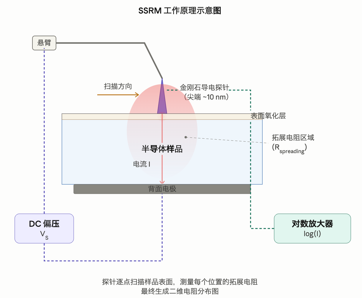
How SSRM works: Use a "pathfinder" to draw a resistance map
In order for everyone to understand more intuitively, let us make an analogy:
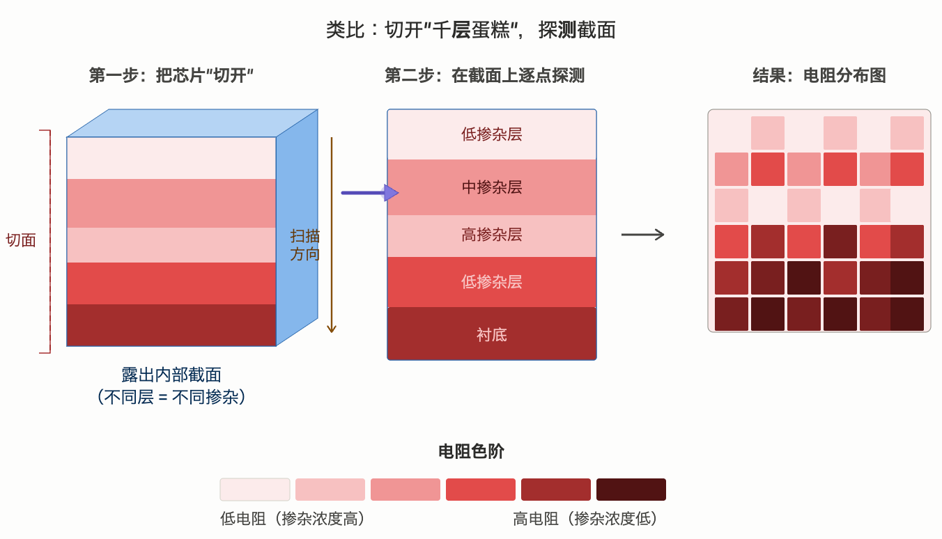
Imagine that there is a piece of "thousand layer cake" in front of you. From the outside, it is just an ordinary whole. But if you cut it in the middle, you can see the layer-by-layer structure on the cross-section - cream layer, cake layer, fruit layer, the layers are different. At this time, you take a probe and poke it point by point from top to bottom on the cut section, and you can feel the difference in softness and hardness of each layer, and finally draw a "section material distribution map".
SSRM does something very similar - first cut the chip sample to expose the internal cross-section. Then use a diamond conductive probe with a tip of only a dozen nanometers to scan the cross-section point by point. What you feel is not the softness or hardness, but the "easiness of conduction" (i.e. resistance) of the material. What is finally obtained is the resistance distribution map of each layer and each area inside the chip.
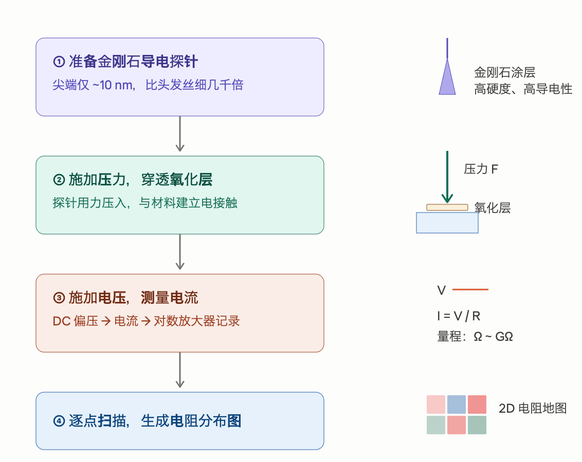
first step: Prepare probe. SSRM uses an AFM probe coated with a conductive material (usually diamond coating). The probe is very hard and pointed, with a tip radius of only about 10 nanometers—thousands of times thinner than a human hair.
Step 2: Apply pressure to establish electrical contact. The probe presses against the sample cross-section with greater force. Why "press hard"? Because most semiconductor materials have a natural oxide layer or contaminants on their cross-sections, it's like wearing an "insulating coat" on the material. The probe needs sufficient force to penetrate this "coat" and establish reliable electrical contact with the material body.
Step 3: Apply voltage and measure current. A DC voltage is applied between the probe and the back of the sample. Electricity flows from the tip of the probe into the sample—the amount of current flowing depends on the resistance of the material beneath the probe. The resistance is small, the current is large; the resistance is large, the current is small. The device records this current through a logarithmic amplifier, covering an ultra-wide range from a few ohms to billions of ohms (GΩ).
Step 4: Scan point by point to generate an image. The probe scans the sample cross-section line by line, and the resistance value is measured at each position. After the scan is completed, all data points are combined to generate a two-dimensional "resistance distribution map". It is clear at a glance where the conductivity is good and where the conductivity is poor.
There is a key concept here called **"Spreading Resistance"**. The so-called expansion resistance refers to the resistance encountered when the current "spreads" from the extremely small contact point of the probe tip into the entire material. Since the contact area is extremely small and the current lines are highly concentrated just below the probe, the resistance contribution at this location is much greater than other parts. This is why SSRM has ultra-high spatial resolution - the signal it measures is basically the resistance information of a small area directly below the probe.
Why is SSRM important?
In the semiconductor industry, "doping" is one of the core processes for manufacturing chips - by injecting specific impurity atoms (such as boron, phosphorus, arsenic, etc.) into the silicon wafer to precisely control the conductivity of the material in different areas. Small deviations in doping concentration may cause the transistor to fail to turn on, fail to turn off, or perform abnormally.
The value of SSRM is that it can directly "see" the carrier concentration (i.e. doping) distribution on the cross-section of a semiconductor device with nanometer-level resolution, allowing engineers to know whether the doping of each layer and each region meets the design. This is like doing a "CT scan" of the chip, clearly showing the internal electrical structure.
Compared with traditional one-dimensional extended resistance measurement (SRP), the advantage of SSRM is that it does not require oblique cutting of the sample and measures directly on the cross-section; and it generates a two-dimensional image with a much larger amount of information.
Application areas of SSRM
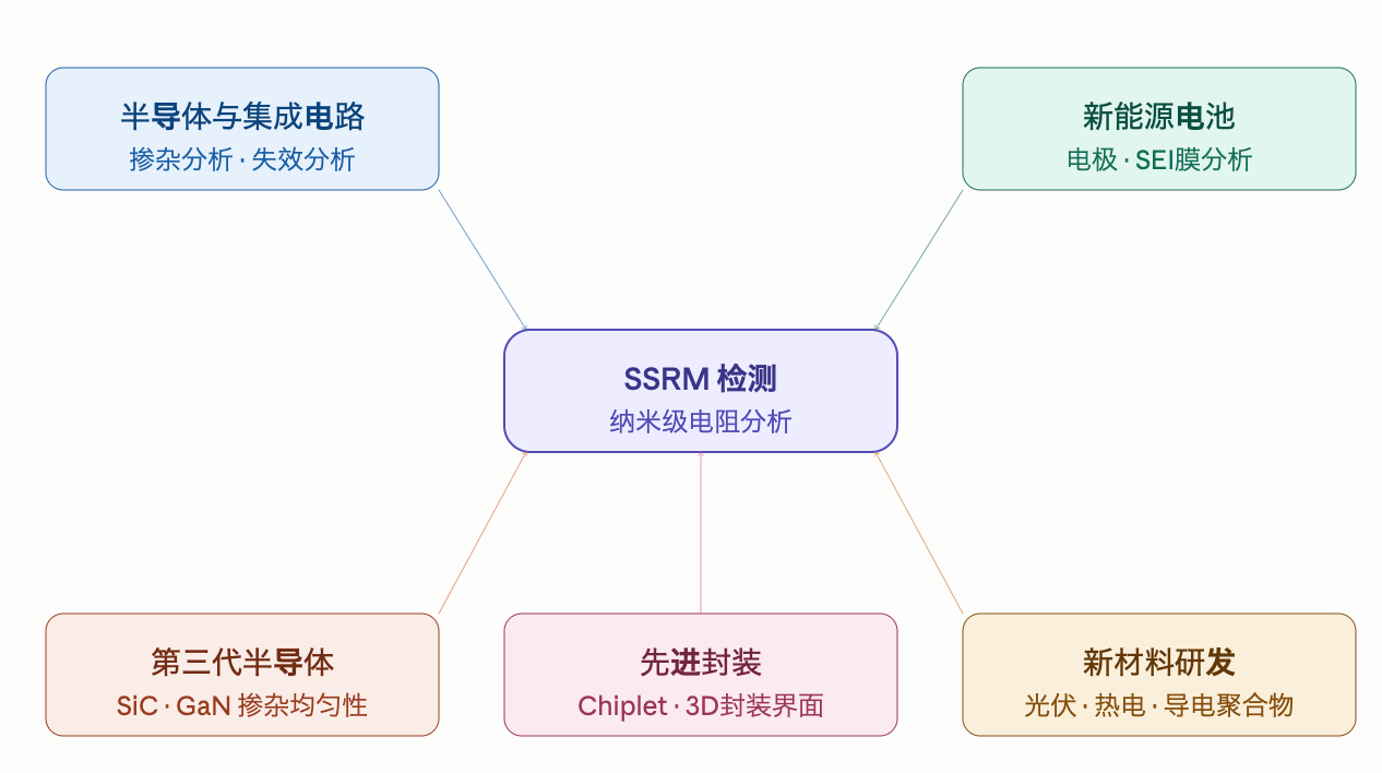
The application scope of SSRM has gone far beyond the initial semiconductor field and plays an important role in multiple frontier industries:
Semiconductors and integrated circuits——This is the most classic application scenario of SSRM. Engineers use SSRM to perform two-dimensional carrier concentration analysis on chip cross-sections for process development, yield improvement, and failure analysis. For example, when a certain batch of transistors has abnormal leakage or threshold voltage deviation, SSRM can accurately locate the region where the doping concentration has deviated, helping to quickly locate the root cause. In advanced process nodes (such as three-dimensional device structures such as FinFET and GAA), two-dimensional or even quasi-three-dimensional carrier distribution information is particularly critical.
New energy battery——SSRM also shows important value in lithium-ion battery research. It can image the resistance distribution of the cross-section of the electrode material, help researchers observe the electrical contact between active materials, conductive agents and binders, evaluate the electronic resistivity distribution of the solid electrolyte interface (SEI) film, and provide microscopic electrical information for optimizing battery performance.
third generation semiconductor materials——Wide bandgap semiconductor materials such as silicon carbide (SiC) and gallium nitride (GaN) are increasingly used in power devices and radio frequency devices. SSRM can be used for doping uniformity assessment and device cross-section analysis of these materials, providing support for material quality control and device process optimization.
Advanced packaging and heterogeneous integration——With the development of chiplet and 3D packaging technology, the demand for electrical property analysis at the interface of different materials is increasing. SSRM enables high-resolution characterization of resistance changes at these interfaces.
Scientific research and development of new materials——In the research of new materials such as photovoltaic materials, thermoelectric materials, and conductive polymers, SSRM can also provide nanoscale electrical information to assist researchers in understanding the microscopic conductive mechanism of materials.
Guozhiwei SSRM platform has recently been upgraded
Finally, I would like to share some good news with you:
ourThe SSRM detection platform has recently completed a comprehensive upgrade. With the dual support of hardware optimization and test process improvement, the platform’s dataSignificant improvements in reliability and reproducibility. Whether it is conventional semiconductor doping analysis or electrical characterization of new material systems, the upgraded platform can provide customers withMore stable and accurate test results。
If you have SSRM-related testing needs or technical exchange intentions, please feel free to contact us.

