

How to have your cake and eat it too? From TEM/SEM to eSPM
We are introduced to the two "ultimate eyes" in the field of semiconductor inspection - scanning electron microscope (SEM) and transmission electron microscope (TEM).
In the past few decades, they have helped humans see clearly the microscopic world at the nanoscale and even the atomic level with their ultra-high resolution. At present, the market for TEM and SEM is very mature. According to industry data, the global electron microscope market has reached billions of dollars and occupies an absolute mainstream position in the production lines of major wafer fabs and top laboratories.
However, in this huge and mature micro-representation market, there is a hiddenThe “ultimate pain point” that has never been fully satisfied。
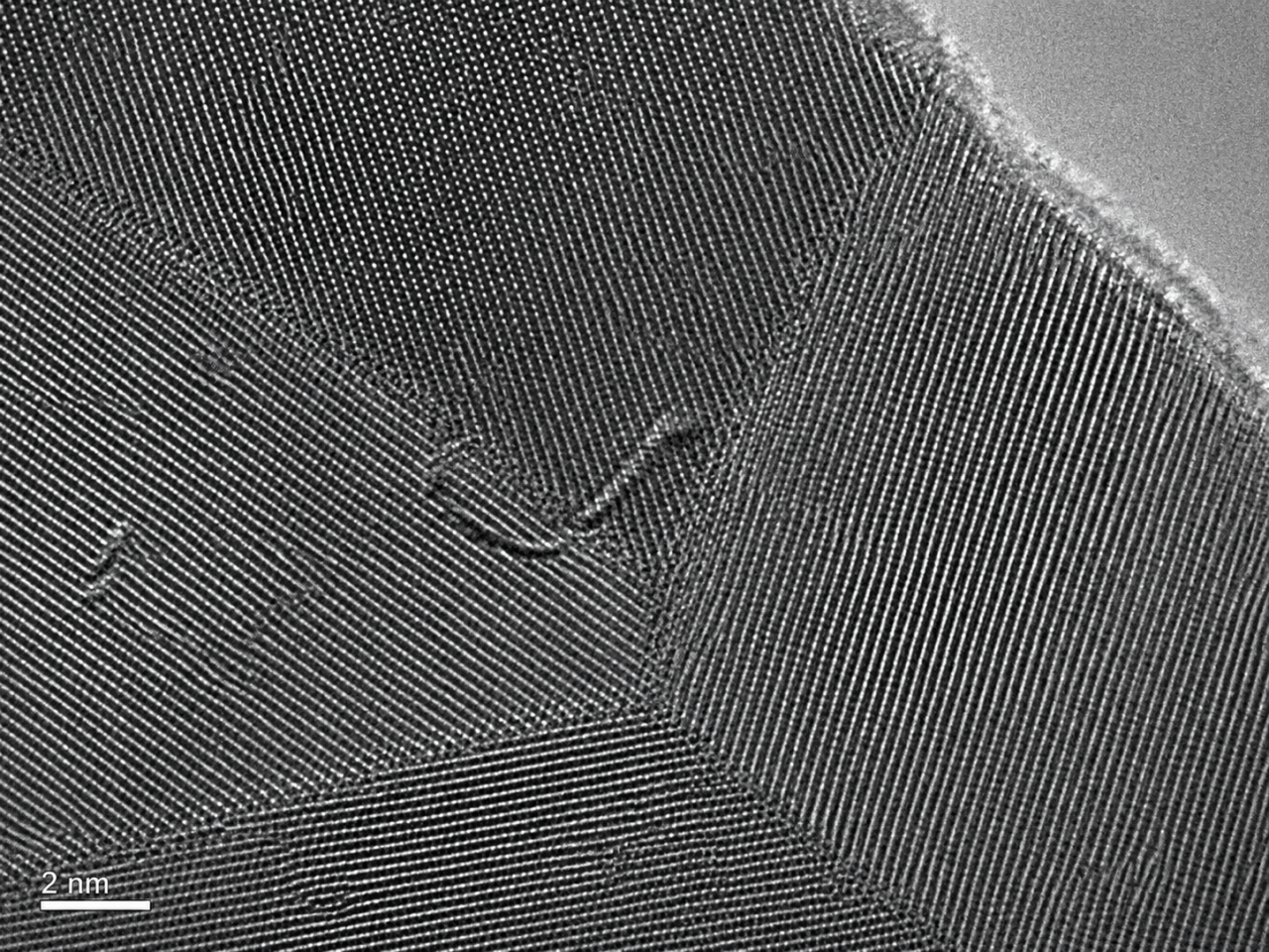
TEM lattice example
01 The choice between fish and bear’s paw: the paradox of structure and electricity
If you use SEM and TEM to inspect advanced semiconductor manufacturing processes, it is like using the highest-definition camera to photograph the architectural frame of a building. Whether the steel bars are straight and the bricks are aligned can be seen clearly with an electron microscope.
But this brings a fatal limitation:You can see its "body" but not its "soul".
For a chip, the "body" is the physical microstructure, and the "soul" is its electrical properties (electricity). In the extremely complex semiconductor manufacturing process, many times the physical structure of the chip seems flawless and the atoms are neatly arranged. However, due to abnormal doping concentration, microscopic leakage current, or extremely small resistance changes, the chip cannot be powered on at all.
This is a typical “can’t have your cake and eat it too” situation in the field of microscopic measurement:Unable to analyze microscopic electrical properties。

Semiconductor failure analysis concept diagram
02 Gray and color: giving “life” to the microscopic world
So, when the electron microscope "cannot see" the electrical properties, what means should we use to detect the microscopic "temper"?
This has led to a new and explosive market in the field of semiconductor inspection - eSPM (Electrical Scanning Probe Microscope).
eSPM is not a single device, but a collective name for a series of technologies that focus on microscopic electrical analysis. The core representatives include:
- SSRM (Scanning Spread Resistance Microscopy): Detect extremely small resistance distribution.
- SCM (Scanning Capacitance Microscopy): Detect the concentration and type of carriers inside a semiconductor.
- SMM (Scanning Microwave Impedance Microscope): Highly sensitive broadband testing of capacitors and resistors.
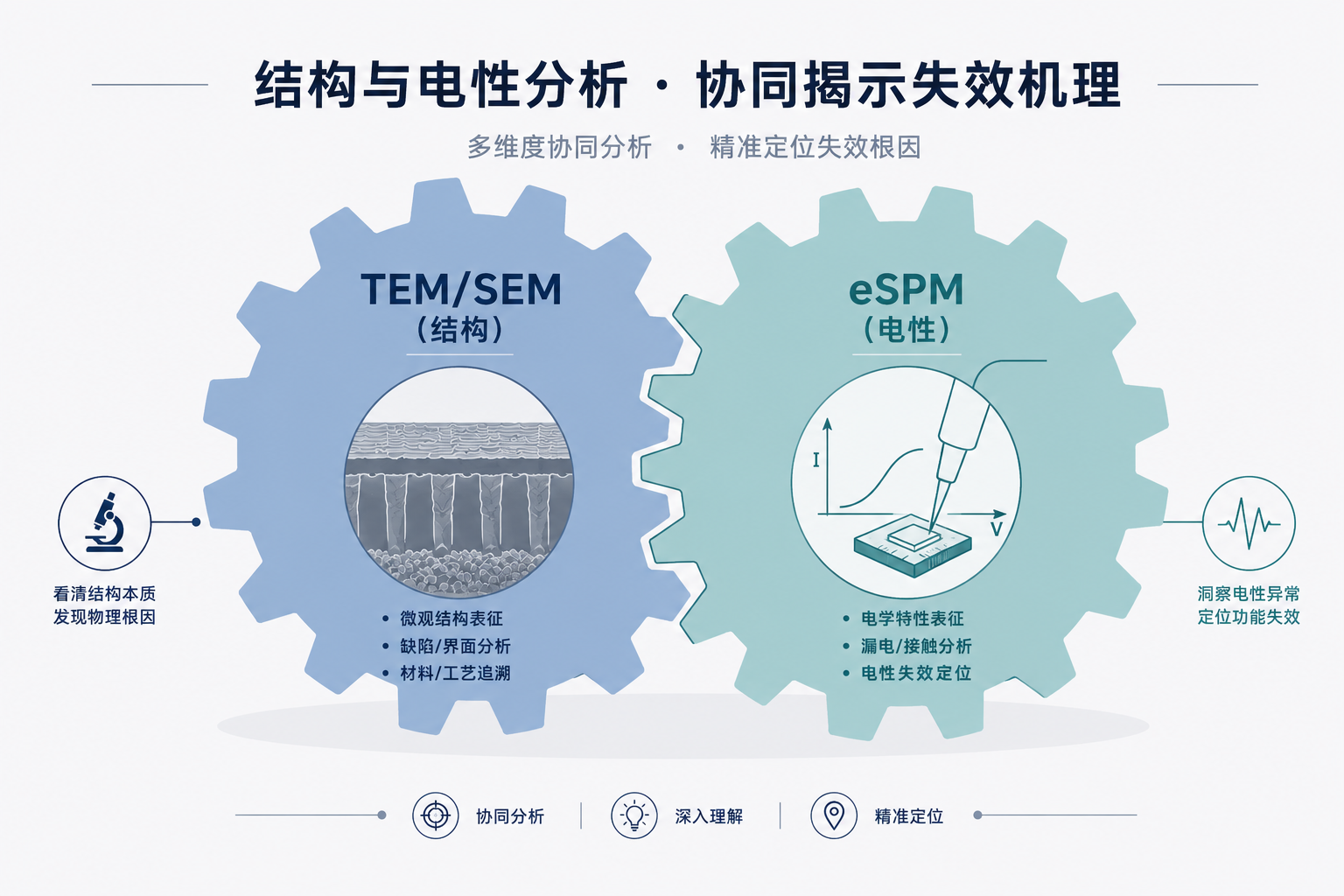
If you compare TEM/SEM and eSPM together, there is a very intuitive visual difference:
The pictures taken by ordinary TEM are usually "grey"; while the pictures scanned by eSPM are often "color".
In the gray and white ultra-high-definition images of TEM, what we see is the cold atomic lattice;
In the colorful spectrum of eSPM (for example, red represents a high-resistance state and blue represents a low-resistance state), what we see is the distribution and flow of live electrons inside the semiconductor. eSPM truly gives "life" to the microscopic world!

Comparison between TEM and eSPM
03 Horsepower cars and smart cars: the ultimate puzzle of the micro-inspection market
Many people may have questions: Is there a relationship of substitution and competition between eSPM and TEM/SEM?
The answer is: definitely not competition, but perfect complementarity.
We can use the familiar "car market" as an analogy:
In the automobile market, there are both traditional performance cars that pursue the ultimate in “horsepower” and mechanical sophistication; there are also new energy vehicles that focus on “electronic interiors” and intelligent experience.
They are both in the huge automobile consumer market, but their specific focuses are completely different. You can't say that smart cars have replaced performance cars, they just meet people's ultimate needs in different dimensions.
The same goes for micro-characterization markets:
TEM/SEM is the "performance car" of the microscopic world. They pursue the ultimate in physical appearance and resolution. This market has been pioneered and is highly mature;
eSPM is a "smart car" in the microscopic world. It focuses on in-depth analysis of electrical characteristics and is a new market with unlimited potential.
In the research and development and failure analysis of advanced semiconductor devices (such as FinFET, GAA transistors, and third-generation semiconductor SiC/GaN), the combination of structural morphology (TEM) + two-dimensional electrical distribution (eSPM) has become an indispensable "golden partner."
It is no exaggeration to say: Wherever there is a demand for testing extreme structures, there must be a demand for testing extreme electrical properties. As big as the existing market for electron microscopy (TEM/SEM) is, so will the future market for eSPM!
From visible atoms to measurable electrical properties; from a gray world to colorful maps. Every leap forward in semiconductor detection technology is pushing Moore's Law forward.
In this tens-billion-dollar microscopic characterization market, the integration and complementarity of structure and electrical properties is the ultimate answer to semiconductor failure analysis.
As a professional team focusing on two-dimensional nanoscale electrical property measurement and imaging,Shanghai Guozhiwei TechnologyexistSMM、SSRM、SCMThe eSPM field has profound technical accumulation and rich practical cases.
If you are also troubled by "invisible" electrical failures inside the chip, please feel free to contact us. Let us work together to take a "color" microscopic electrical map of your chip!

