

The chip is clearly "off", so why is the current still leaking out?
In daily life, electrical appliances usually stop working after the switch is turned off.
But in semiconductor devices, things are not so cut and dry.
Even when the transistor is off, a small amount of current may still flow quietly through the device, bypassing the normal path. This type of current that should not occur, or significantly exceeds expectations, is often calledLeakage current。
The leakage in a single device may be very small, but when hundreds of millions of transistors are integrated inside the chip, the accumulation of small currents may lead to increased standby power consumption, device heating, performance drift, and even reduced reliability.
So, where do these currents "leak" from?
01 There is more than one type of leakage
Think of a transistor as a set of tiny gates controlled by a gate.
Normally, the gate determines whether the current channel is open or closed. However, as device size shrinks, insulation layers become thinner, and electric fields increase, current may "take advantage of" through multiple less-than-ideal paths.
Common leakages mainly include:
Subthreshold leakage
Although the gate voltage has not yet reached the level to officially turn on the device, the channel is not completely closed, and a small amount of carriers still pass through.
It's like the faucet has been tightened, but water drops are still dripping slowly.
Gate oxide leakage
There is usually an extremely thin insulating layer between the gate and the channel. When the insulating layer is too thin, has defects, or is subjected to a strong electric field, carriers may pass through the insulating layer through tunneling.
It's a bit like a wall getting thinner and thinner, and things that couldn't pass through before have a chance to "pass through".
PN junction reverse leakage
There are junctions formed by multiple differently doped regions inside the device. Additional current may also occur in the junction region under conditions of reverse bias, elevated temperature, or many defects.
GIDL
There is another type of leakage that often occurs in the edge area of the gate close to the drain and is caused by a local strong electric field. This is the GIDL that this article focuses on.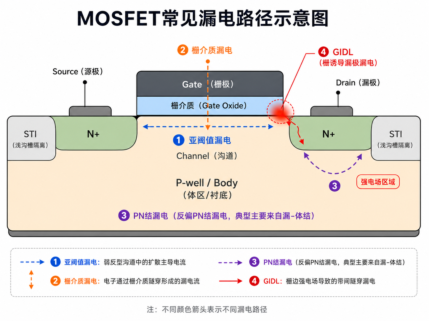
02 GIDL: The gate is closed, but "penetration" occurs at the edge
The full name of GIDL isGate-Induced Drain Leakage, Chinese is usually calledGate induced drain leakage。
Taking NMOS in the off-state as an example, when the drain voltage is high and the gate voltage is low or even negative, a strong local electric field will be formed near the edges of the gate and drain.
Under the action of a strong electric field, the energy bands inside the semiconductor are significantly bent, and some electrons may directly enter the conduction band through inter-band tunneling. Subsequently, the electrons are collected by the drain, and the corresponding holes flow to the substrate or body region, thereby forming additional leakage current in the off state. Classic studies attribute a significant source of GIDL to band-to-band tunneling in the deep depletion region near gate-drain overlap; interface traps may also further amplify leakage through trap-assisted tunneling.
In other words, normal current should pass through the channel in the middle of the device, while GIDL is more like the current finding an "abnormal shortcut" from the edge of the gate.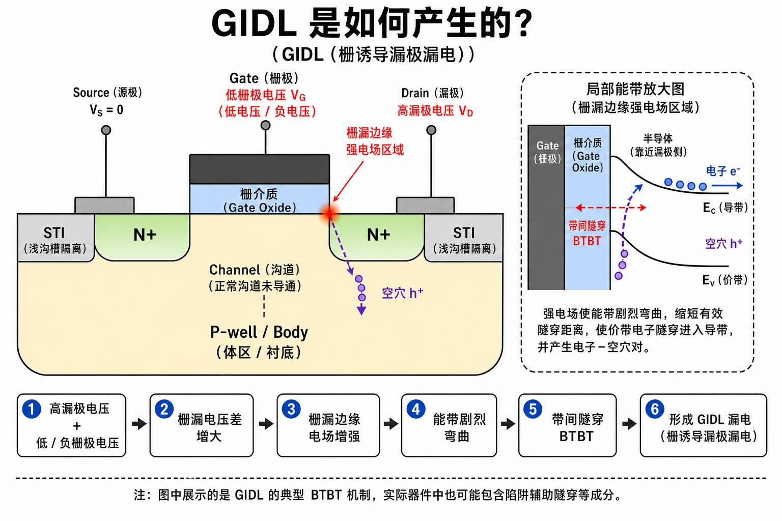
What conditions may aggravate GIDL?
Usually you need to pay attention to:
The voltage difference between gate and drain;
The local electric field at the gate-drain edge;
Drain doping and junction structure;
Gate insulation layer and interface defects;
The electrical stress and process fluctuations experienced by the device.
However, we only see the abnormal leakage curve and cannot directly declare that "the murderer is GIDL". Semiconductor failure analysis is not a mystery novel, and you cannot immediately close the case when you see a suspicious character.
03 To know the leakage of the device, you also need to know “where the leakage is”
Routine electrical testing can tell us:
The device did experience abnormal leakage.
But it may not directly tell us:
Which tiny area is the anomaly located in and what defect is caused by it?
It's like the water meter at home showing abnormal water consumption, but being unable to pinpoint which water pipe has a crack.
Therefore, leakage analysis often needs to go through three levels:
Step 1: Narrow down the range based on electrical characteristics
Through I-V curves, different gate and drain bias conditions, and necessary temperature tests, it can be initially determined whether the leakage is closer to sub-threshold, junction region, gate dielectric or GIDL mechanisms.
Step 2: Find local leakage locations
CAFM, that isconductive atomic force microscope, can use a conductive probe to scan the sample surface, and obtain the surface morphology and local current distribution at the same time under appropriate sample preparation and bias conditions.
If the current in an area is significantly higher than the surrounding area, it may appear as a "hot spot" on the current map. Local I-V measurements can then be performed at designated locations to further compare conductivity differences between normal and abnormal areas.
CAFM has been applied to the analysis of semiconductor leakage, contact anomalies, and dielectric breakdown. Guozhiwei Technology's high-sensitivity CAFM service also caters to testing needs such as local small current, insulation film breakdown, and nanoscale electrical distribution.
Conventional electrical testing answers "Is there any leakage?", while CAFM is closer to answering "Where is the leakage?"
Step 3: Find the root cause from the cross section
After finding the abnormal location, you need to further confirm whether it exists in the surrounding area:
Abnormal film thickness or interface;
Abnormal gate edge structure;
Crystal defects or local damage;
Abnormal doping, carrier or resistance distribution.
At this time, FIB can be used to prepare fixed-point cross-sections of the target area, and then combined with SEM, TEM, etc. to observe the microstructure; SMM, SSRM, SCM and other electrical scanning probe technologies can also be used according to the problem to analyze the local impedance, resistance and carrier distribution of the cross-section.
Guozhiwei Technology currently provides CAFM, SMM, SSRM, SCM, AFM, as well as FIB, SEM-EDS, TEM-EDS and other analysis methods. Its business covers device physical failure analysis, electrical failure analysis and nanoscale two-dimensional electrical imaging.
When customers needQuickly and intuitively see the PN junction morphology, when you need to submit a report that meets common industry standards and has extremely beautiful images,Mature SCM scanning capacitor SMM scanning microwave is the best choice。
When customers face extremely complex advanced processes or need to extractMulti-dimensional material impedance information, it is necessary to carry out the micro-regionWhen accurate qualitative analysis of doping concentration is required, accurate SSRM scanning extended resistor can provide powerful fire support.
Many times, advanced failure analysis laboratories will useSCM/SMM confirms PN type + SSRM further confirms SCM/SMM test results and provides sub-resolutioncombination. Only by bridging the two can the leakage and doping anomalies hidden deep in the nanometers be hidden.
04 Leakage analysis is not about “guessing the answer” with one device
For complex devices, a complete leakage analysis usually requires the formation of a chain of evidence:
Electrical test found abnormality
↓
Judging possible mechanisms based on bias characteristics
↓
Finding abnormal areas using local current imaging
↓
Perform fixed-point cross-section analysis on the target location
↓
Combine structure, carrier and resistance distribution to verify root cause
CAFM, FIB, TEM, SMM or SSRM are not substitutes for each other.
They are more like an analysis team with a clear division of labor:
Electrical testing is responsible for finding problems;
CAFM is responsible for looking for local abnormal currents;
FIB is responsible for accurately reaching the target cross-section;
SEM and TEM are responsible for observing the structure and interface;
SMM, SSRM, and SCM are responsible for supplementing local electrical and carrier information.
Really valuable failure analysis is not just about taking a beautiful picture, but also aboutAbnormal electrical properties, spatial location and physical causesCorrespond.
Turn invisible leakage into data that can be analyzed
Leakage in semiconductor devices often occurs at the micron or even nanometer scale.
It may come from a local defect, an abnormal doping distribution, or from the increasing electric field at the gate-drain edge. It is often difficult to make accurate judgments only by relying on macroscopic electrical curves.
Shanghai Guozhiwei TechnologyFocusing on the analysis and testing of semiconductor chips, focusing on scanning probe microscopy and electron microscopy analysis technology, it can based on the sample structure, failure phenomenon and analysis objectives,Combination of CAFM, SMM, SSRM, SCM, FIB, SEM and TEM, etc.Analysis methods provide targeted testing and analysis solutions for device leakage, dielectric failure, doping anomalies and micro-area electrical problems.
From discovering leakage, to locking the location, to verifying the root cause, abnormalities in the micro world no longer remain a matter of speculation.

