

There is an "invisible map" in the chip: understanding SCM scanning capacitance microscopy
A chip was judged to have failed during the testing process: the leakage exceeded the standard, or the threshold voltage was inexplicably off.
The engineer followed the standard process - FIB sectioning, SEM photography, TEM viewing of the crystal lattice, and EDS composition. The results were all normal: the gate oxide was intact, the contact holes were unobstructed, the metal layer was regular, and the composition was not abnormal.
I can't fault anything structurally, but the device just doesn't work.
The problem often lies in a place "invisible" to the electron microscope——Doping。
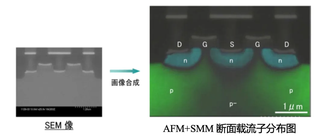
[SMM dc/dv (SCM) + SEM composite image]
01 "Invisible map" in the chip
The reason why a chip can work depends on more than just those trenches, gates and metal lines. What really turns the transistor on and off are the impurities doped into the silicon - elements such as phosphorus, boron and arsenic, which are distributed in different concentrations in different areas to form N-type and P-type regions. The junction between the two is the PN junction.
The structure determines "where the part grows", and the doping determines "what the part is".
The trouble is that the dopant atoms are only sporadically embedded in the silicon crystal lattice. It does not change the morphology and hardly changes the contrast - so under an electron microscope, an abnormally doped area and a intact area look exactly the same.
The traditional approach on the production line isAcid corrosion dyeing: Soak the cross section with chemical reagents. Different doped areas will corrode at different rates, and the location of the junction will be revealed. Low cost and quick to use, it is still a commonly used primary screening method. But the amount of information is limited - you can only see "there is a knot here", you can't tell the concentration, and you can't distinguish between N-type and P-type. The repeatability is not ideal yet.
To truly draw this "invisible map", we need to use another method.
02 SCM: Turn the probe into a nanoscale capacitor
Scanning Capacitance Microscopy (SCM)The idea is actually quite straightforward.
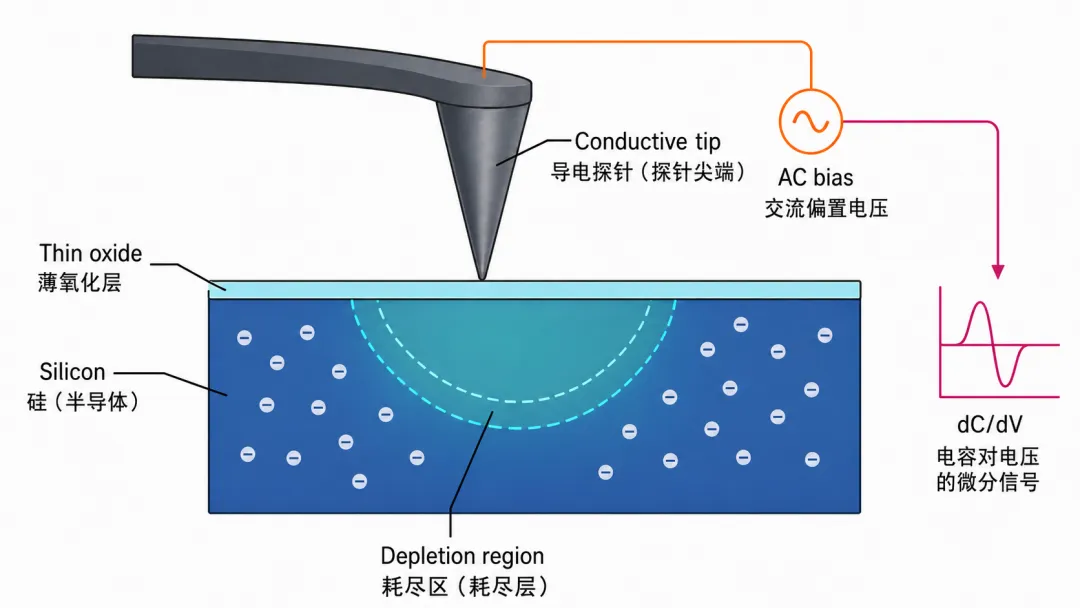
An extremely sharp conductive probe is pressed against the surface of the sample. The probe tip, the thin oxide layer on the surface, and the silicon below-these three exactly form aMOS capacitors shrunk to the nanometer scale. The most classic C-V (capacitance-voltage) behavior in semiconductor physics also holds true in this region as small as tens of nanometers.
Next apply an AC voltage to the probe. The carriers in silicon will be repeatedly driven out and put back by this voltage. The depletion layer on the surface expands and contracts like breathing, and the capacitance changes accordingly. What SCM measures is this rate of change (dC/dV), and there are two key pieces of information hidden in this signal:
Phase → Type of carrier. The C-V curves of N-type and P-type change in opposite directions with voltage, so you can tell whether the phase is an electron or a hole at a glance, which is very clean and neat.
Amplitude → carrier concentration. The lower the concentration, the greater the "breathing" amplitude of the depletion layer, and the stronger the signal; the higher the concentration, the weaker the signal.
The probe sweeps across the cross section point by point, and a complete two-dimensional carrier distribution map comes out. The effective detection range of SCM roughly covers 10¹⁵ to 10²⁰ atoms/cm³ - the lower limit can cover the background concentration of the wafer substrate, and the upper limit can cover the heavily doped region of the source and drain of the MOS tube, which happens to be the section of the device that needs to be seen clearly.
[SCM principle diagram]
An off-topic piece of trivia:The prototype of SCM was not born in a semiconductor laboratory, but from a failed home video player. In the early 1980s, RCA introduced the CED VideoDisc, a disc system that relied on a stylus to read changes in capacitance to play video. It was a commercial failure. But its extremely sensitive capacitance pickup circuit was used by engineers J. R. Matey and J. Blanc to make a scanning capacitance microscope, which was published in the "Journal of Applied Physics" in 1985. Forty years later, a consumer electronics solution that was eliminated by the market has become a key tool for advanced process analysis.
03 What are the four pictures in the report talking about?
This is the confusion that many people have when they get the SCM report for the first time: Why are there four pictures?
Because the output of SCM is naturally a "four-piece set", each one performs its own duties and each one is indispensable:
① Topography - first check whether the data is credible
This picture does not contain electrical information, it records the ups and downs of the cross section. Its function is to check the quality of sample preparation: whether the surface is flat enough, whether there are scratches and residues. If the topography map is in a mess, the credibility of the next three images will be questionable. **This is the first step to judge the quality of a SCM report, and it is also the most easily ignored one.
② Amplitude diagram (Amplitude) - find where the PN junction is
The lower the concentration, the stronger the signal, so near the PN junction (the transition region where carriers are depleted), the amplitude signal will form an obvious bright band. If you want to know how deep the knot is and how far it spreads laterally, look at this.
③ Phase diagram (Phase) - distinguish between N type and P type
The phase has only two positive and negative states, corresponding to electrons and holes, and the boundaries are clean and neat. Regions without carriers (such as oxide layers, metals) are noise on this map.
④ SCM Data——Comprehensive picture, also the core one
Composite type and intensity together, usually rendered in false color. The more popular color matching in the industry is:Red represents the N-type, purple represents the P-type, and green represents the PN junction and carrier-free region.. The doping layout of the entire device can be seen clearly in this picture.
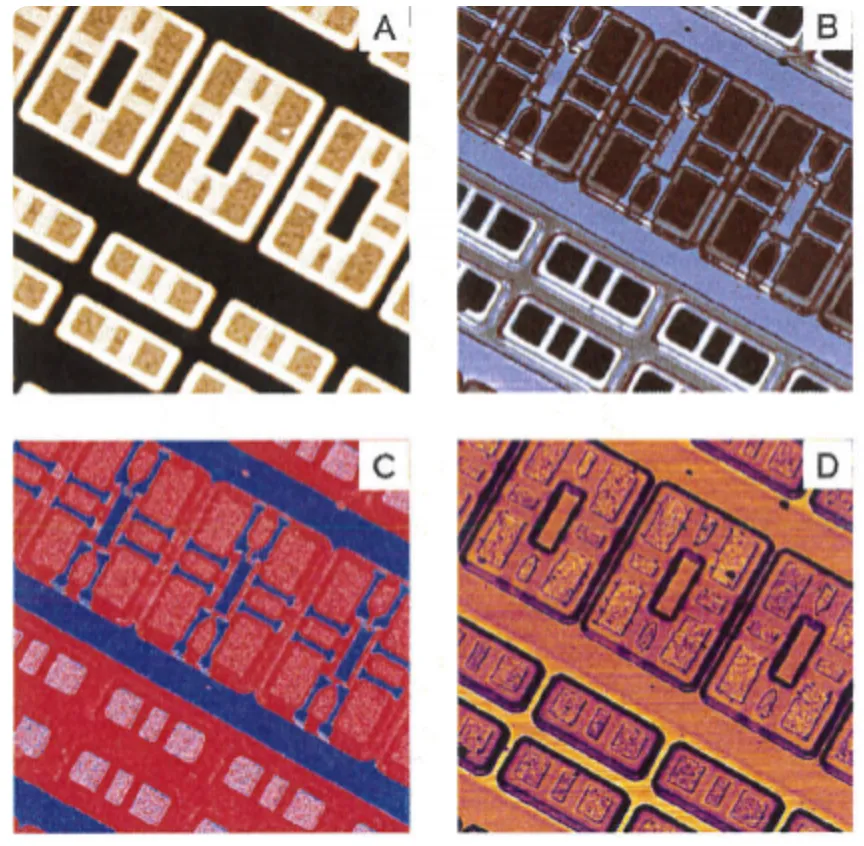
[A: Morphology | B: dC/dV amplitude | C: dC/dV phase | D: Capacitance]
Source: https://afm.oxinst.cn/outreach/SCM
Looking at the four pictures together, the logic is as follows:First confirm that the data is credible (morphology), then locate the junction (amplitude), then determine the type (phase), and finally synthesize the complete layout (SCM Data)。
04 When should I take SCM?
Combined with the actual needs of the production line and laboratory, SCM is often the most efficient choice in the following scenarios:
Process development and validation.After ion implantation and annealing, how deep is the junction depth? Is lateral diffusion beyond design? Are the measured two-dimensional distribution and process simulation consistent? SCM can give direct image evidence rather than indirect inference.
Yield anomalies and failure analysis.When problems such as leakage, threshold drift, and device failure to turn on occur, and FIB/SEM/TEM all show that the structure is normal, doping anomalies are the key suspects. SCM is currently one of the few methods that can directly image it.
Power devices and compound semiconductors.The epitaxial layer concentration and terminal structure of SiC and GaN are the key to withstand voltage and reliability; the same is true for the photodiode doping profile of CIS, which requires two-dimensional distribution data the most.
Reverse engineering and competitive product analysis.The structure can be restored by TEM, but the doping scheme cannot—that’s where the process know-how really hides.
As forWhen not to attend SCM:If you just want to confirm "where the knot is approximately", acid etching and dyeing is faster and cheaper; if you want the absolute value of the longitudinal concentration of the entire wafer, SIMS is more suitable. What’s irreplaceable about SCM is nanometer-scale spatial resolution—it can tell you what’s happening in a specific corner of a specific transistor.
The boundary must also be made clear: signal and concentration have a non-linear relationship and are affected by the sample preparation state, so what SCM is good at isQualitative judgment and relative comparison(Here is denser than there, N-type here, P-type there, where is the junction), rather than a precise value of absolute concentration. It is extremely sharp when used in the right place, but it is easy to be disappointed if you have wrong expectations.
04 When should I take SCM?
SCM is very different from TEM.
TEM sample preparation has relied heavily on FIB automation, with standard processes and reproducible results.However, SCM does not have such a shortcut so far.. What it requires is an ultra-smooth, almost damage-free cross-section, plus the precise growth of a high-quality thin oxide layer on this cross-section - the former relies on manual grinding and polishing, and the latter relies on the control of oxidation conditions.
This means that the success or failure of SCM depends largely on "craftsmanship": if the same sample is made by different people, one picture may be clean and the other may be full of noise. This is why SCM has clear principles and clear value, but it has never been popularized in every laboratory like TEM.
You can buy equipment, but you can’t buy experience.. For most teams, it is a more cost-effective option to hand over this matter to a third-party laboratory that is experienced in doing it.
Shanghai Guozhiwei TechnologyHe has long been focused on nanoscale electrical analysis, has complete sample preparation and data analysis capabilities of SCM, and masters eSPM methods such as SMM, SSRM, and C-AFM. Whether you need a clear picture of the PN junction topography or a complete carrier distribution analysis solution, we can match the right path for you.
Being able to see the structure is only the first step; only by understanding the electrical properties can you truly find the problem.
Welcome to contact us to chat about the samples you have.

