

Anatomy Lesson of a Laser Chip: Structure, Design Difficulties, and Those "Invisible" Parts
Today, with the explosion of AI computing power, the amount of data flowing between data centers per second is rising at an alarming rate. 1.6T optical modules, CPO (co-packaged optics), and silicon photonics integration have become the hottest keywords in the entire optoelectronics industry. But no matter how the architecture evolves, there is always a chip as small as a fingernail or even smaller at the front end of the link——Semiconductor laser. It is responsible for turning electricity into light. Its efficiency, wavelength stability and lifetime almost determine the upper limit of an entire optical link.
What does this chip look like? What makes it difficult to do? And - how do engineers "see" whether the structure they designed has actually been built?
01 First distinguish between two types of lasers
Semiconductor lasers are divided into two categories based on "where the light comes from."
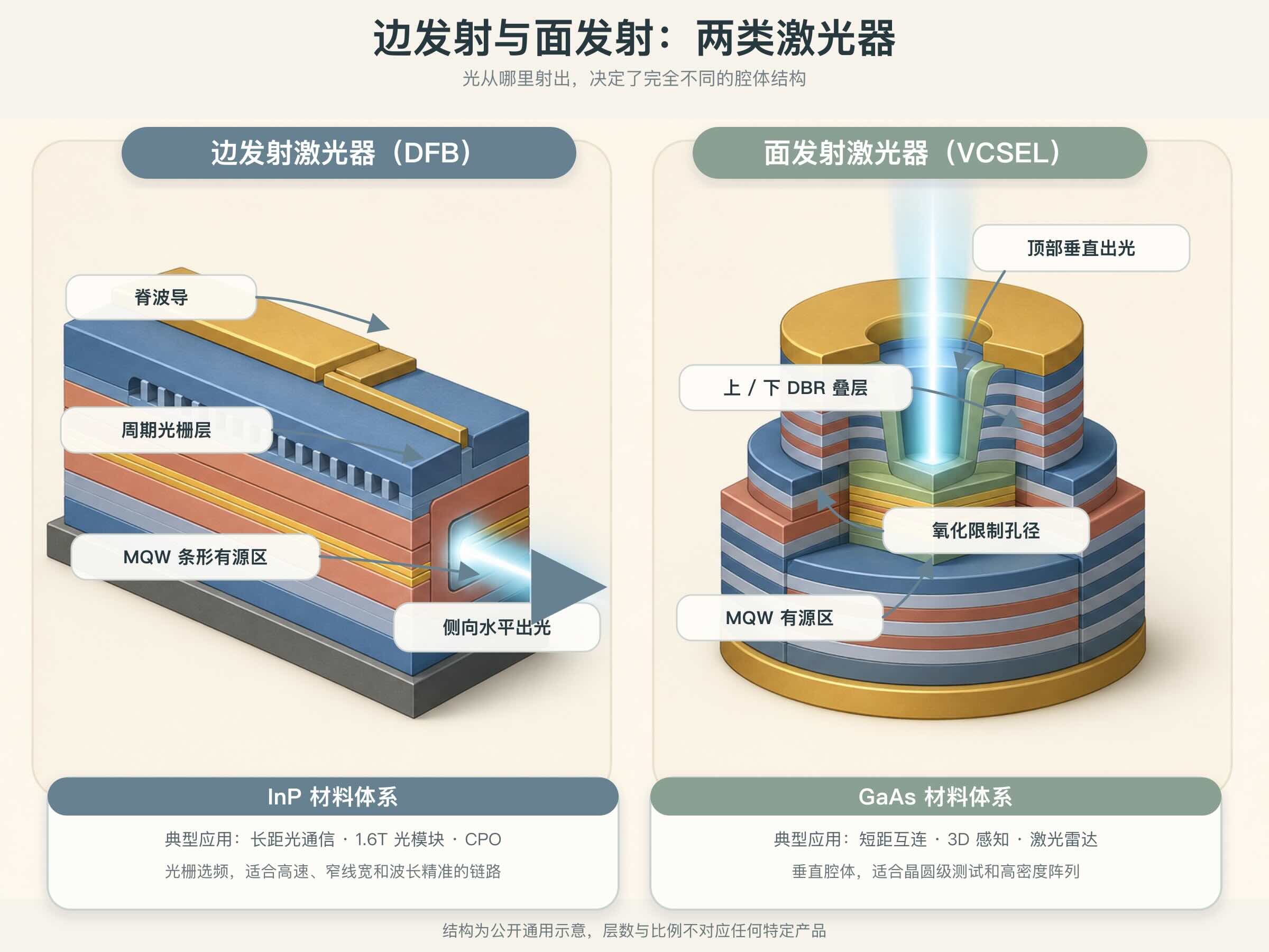
Edge emitting laser (EEL):Light is emitted from the side of the chip (the cleavage cavity side). It is divided into several types internally. The FP laser has the simplest structure, relying on the cleavage surfaces at both ends of the chip as reflectors, and the wavelength is not pure enough; the DFB laser has a very fine grating engraved next to the active area, allowing only a specific wavelength to get feedback, so the wavelength is very pure, and it is the absolute main force in long-distance optical communication; EML goes a step further, and makes the DFB and an electroabsorption modulator on the same chip - the laser continuously emits light, and the modulator is responsible for rapid "switching", thereby supporting high-speed transmission of tens or hundreds of Gbps. The material system of this type of device is usually InP.
Surface emitting laser (VCSEL):Light emerges vertically from the front of the chip. It does not split the cavity surface, but stacks dozens of layers of reflectors (DBR) above and below the active area to form a resonant cavity. VCSEL can be densely arranged on the wafer and tested on the whole chip. It has obvious advantages in cost and consistency. It is widely used in short-distance interconnection in data centers, 3D face recognition in mobile phones and vehicle-mounted lidar. The material system is usually GaAs.
One sentence summarizes the division of labor:Edge emission is used for long-distance, high-speed, and accurate wavelength applications; VCSEL is used for short-distance, high-volume, cost-effective, and array-based applications.
02 Take apart a DFB chip and look at it
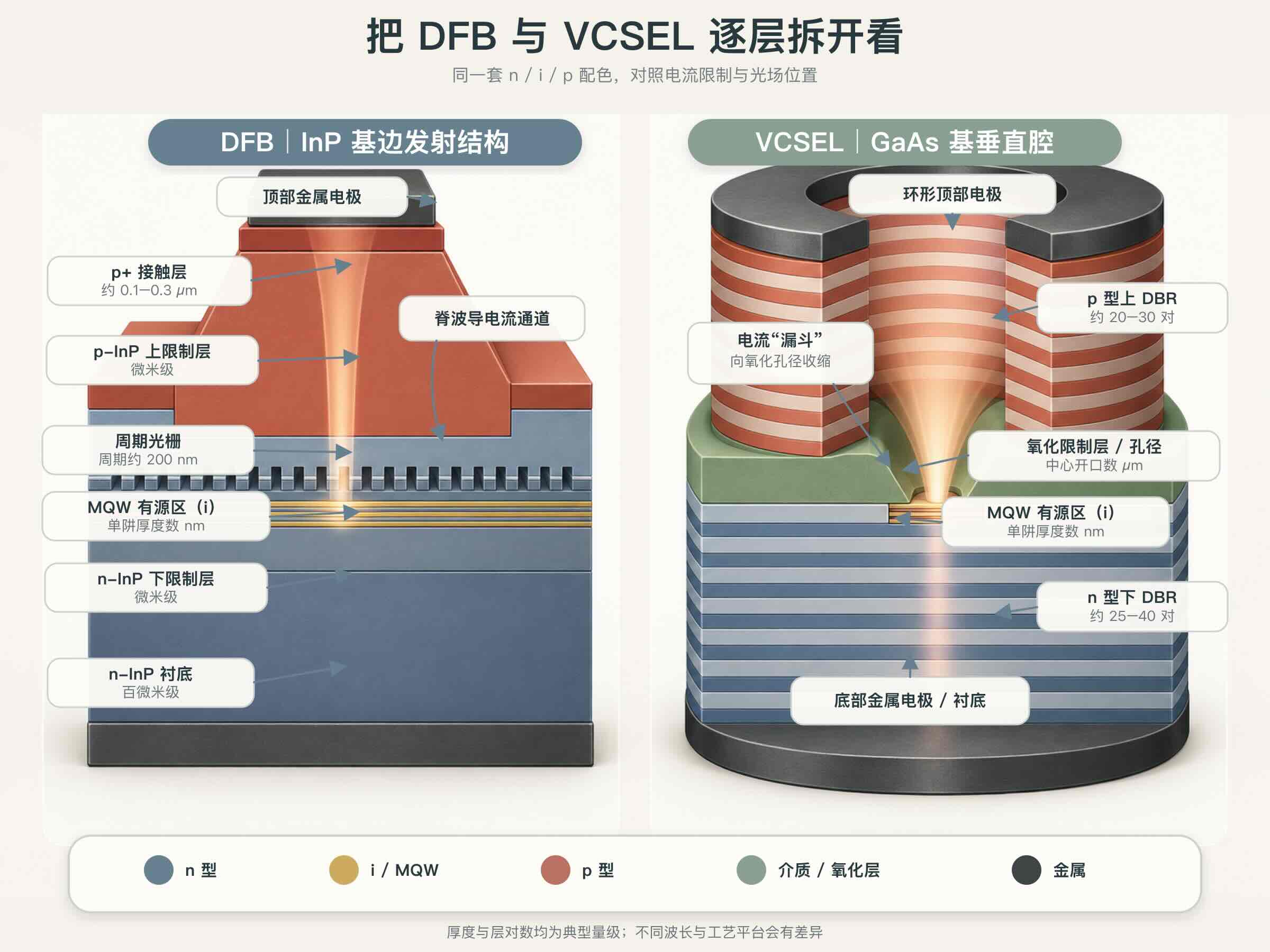
The laser chip is not a uniform piece of material, but a sandwich "grown" layer by layer through epitaxial growth. The total thickness is often only a few microns. Taking an InP-based DFB as an example, from bottom to top it is roughly:
n-type InP substrate and lower confinement layer——Provide electrons, and at the same time, because the refractive index is lower than the central area, the light is "sandwiched" in the middle to prevent it from escaping.
Multiple quantum well active region (MQW)——The heart of the entire chip. It is composed of several alternating layers of ultra-thin materials with a thickness of only a few nanometers. It "locks" electrons and holes into these layers at the same time, allowing them to recombine and emit light efficiently in a very small space. The thickness and composition of the well directly determine the emission wavelength, and the error tolerance is extremely low.
grating layer——A periodic undulating structure with a period usually on the order of more than two hundred nanometers. Its function is to only allow a certain wavelength to receive positive feedback, thereby "locking" the laser spectral line in an extremely narrow range.
p-type InP upper confinement layer and p+ contact layer——Provide holes and form low-resistance contact with metal electrodes.
current limiting structure——This step determines whether the current flows honestly only through the center of the active area. A common approach is to make the active area into a narrow ridge (ridge waveguide), or to grow semi-insulating material on both sides to "block" the current in the middle (buried heterojunction).
The layer structure logic of VCSEL is similar, but more extreme: its upper and lower DBRs are each composed of twenty or thirty pairs of thin layers with alternating refractive index. The thickness of each layer must be accurate to a quarter of a wavelength; there is also a layer above the active area formed by wet oxidation of a material with extremely high aluminum content.Oxidation limited pore size, a conductive window only a few microns in diameter remains in the center, confining both the current and the light field.
03 Five really difficult things
Drawing the structure only requires a picture, but making it is another matter.
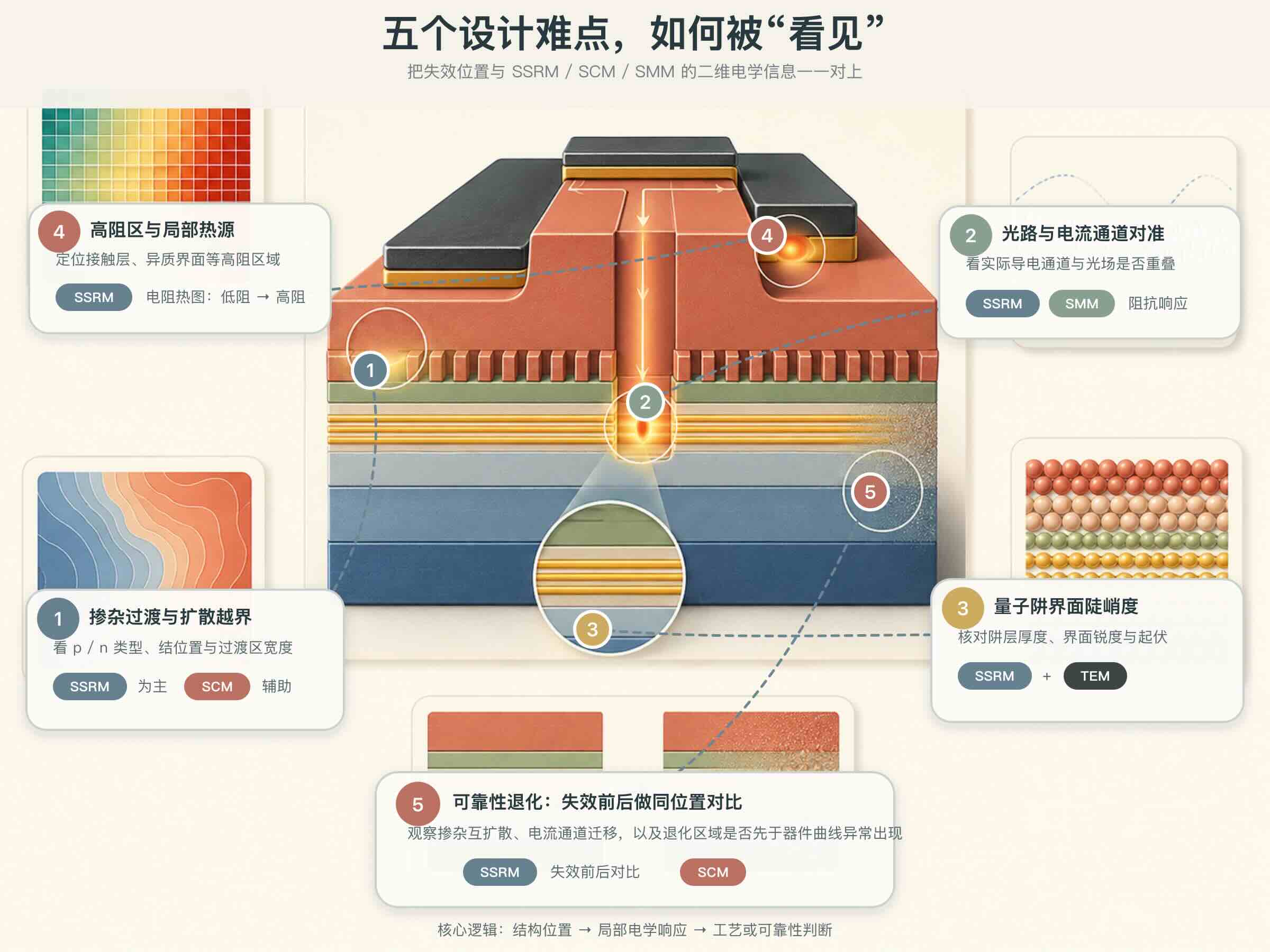
Difficulty 1: The doping profile must be "stuck" in the correct position.The confinement layer needs to be doped high enough to reduce the resistance, but once the dopant atoms diffuse into the active area, they will become non-radiative recombination centers - when the current goes in, heat instead of light comes out. The p-type dopant commonly used in the InP system has a strong diffusion ability and a very narrow process window; in a buried structure using a semi-insulating barrier layer, there is also the classic problem of interdiffusion between the barrier layer and the p-type dopant, resulting in a leakage channel.A clean line on the design drawing is often a blurred transition zone in reality.
Difficulty 2: The path of light and the path of electricity must be aligned.The efficiency of the laser depends on the degree of spatial overlap between the "injected current" and the "light field distribution". The depth of the ridge waveguide etching differs by tens of nanometers, the lateral growth morphology of the buried junction is slightly different, and the diameter of the oxidized aperture of the VCSEL is off by half a micron - the current will bypass the area with the strongest light field, or current convergence will occur at the edge. This is one of the most common sources of yield fluctuations.
Difficulty three: The quantum well interface must be steep enough.In a well layer that is several nanometers thick, if there are composition gradients or fluctuations at the interface, the luminescence wavelength will shift and the spectral lines will broaden. This puts forward almost stringent requirements on the control accuracy of epitaxial growth.
Difficulty 4: Resistance and heat are a dead end.Holes have naturally lower mobility than electrons, and the series resistance on the p-type side is always a heat generator. VCSEL is more typical: DBR serves as both a reflector and a current channel, and each heterogeneous interface has energy band spikes that block carriers. Increasing doping can reduce resistance, but it will increase optical loss due to free carrier absorption; lowering doping can reduce loss, but resistance and heat generation will increase.All engineers can do is to make gradual transitions and modulated doping at the interface to find a balance point between the two curves - and whether this balance point really falls on the design value cannot be answered by electrical testing alone.
Difficulty five: Reliability degradation occurs in invisible places.After the device ages, catastrophic optical damage may occur on the cavity surface, dark line defects may appear in the active area, the doping profile may drift due to long-term high temperature and high current, and the electrode metal may diffuse inward. These changes often occur at the nanometer scale before the inflection point in the current-optical power curve appears.
04 How to "see" these difficulties
The five difficulties above have one thing in common:They all occur on nanoscale cross-sections, and are directly related to "where the carriers/doping are distributed."Conventional electrical testing can only give a device-level ledger. Methods such as SIMS can give a longitudinal profile in the depth direction, but cannot give a two-dimensional spatial distribution. This is where scanning probe-type electrical characterization comes in.
SCM (Scanning Capacitance Microscopy)The imaging is performed by changing the capacitance between the probe and the sample with the bias voltage. It is extremely sensitive to the carrier type and can clearly outline the positions of the p-region, n-region and pn junction interface. It is suitable for quickly answering "Where is the knot and is it the right type?"
SSRM (Scanning Spread Resistance Microscopy)A conductive diamond probe with a bias voltage is used to contact the sample cross-section, and the extended resistance under the tip is measured to quantitatively map the carrier concentration distribution. Its lateral resolution can reach the nanometer level, and the carrier concentration it can cover spans a wide range of 10¹⁵ to 10²¹ cm⁻³. It is currently the best method for balancing resolution and dynamic range in two-dimensional carrier quantitative analysis. The trade-off is extremely demanding cross-sectional sample preparation.
SMM/SMIM (Scanning Microwave Impedance Microscopy)Sensing local impedance through microwave reflection signals, the contact pressure is small, the damage is low, and it is equally sensitive to dielectric materials - which makes it uniquely valuable when observing "dielectric and semiconductor coexistence" structures such as oxidation-limited pores.
Corresponding to the previous five difficulties:
Design difficulties | Main means of representation | what do you want to see |
Doping Profiles and Diffusion Transgression | SSRM is the main one, SCM is the auxiliary one. | Concentration transition width from limiting layer to active area, whether it crosses the boundary |
Optical path and circuit alignment | SSRM、SMM | Actual conductive channel locations, oxidized pore boundaries on cross-section |
Quantum well interface steepness | SSRM + TEM combination | Actual thickness of well layer and interface sharpness |
Series resistor and heat source | SSRM | Positioning of high-resistance areas such as DBR interfaces and contact layers |
reliability degradation | SSRM/SCM comparison before and after failure | Doping interdiffusion and changes in current channels |
As an analysis service provider focusing on the measurement and imaging of two-dimensional nanoscale electrical properties, Guozhiwei has complete integration capabilities in the above scenarios.
We independently developedHigh sensitivity and high vacuum SSRM module: Using a diamond-coated probe, the lateral resolution can be on the order of 1nm to tens of nanometers, and the resistance detection range covers 10⁴–10¹² Ω. The self-developed high vacuum environment eliminates the adsorption of water vapor and impurities in the air on the sample surface, which significantly improves the stability and quantitative credibility of the measurement.
At the same time, we have a variety of electrical modes such as SCM, SMM/SMIM, and C-AFM, as well as the combined capabilities of FIB, SEM-EDS, and TEM-EDS. From cross-sectional sample preparation, structural morphology confirmation to electrical quantitative analysis, it can be completed in a closed loop within the same technical team. For devices such as lasers, which have extremely thin structures, numerous interfaces, and extremely hidden failures,The quality of sample preparation often determines the success or failure of the results more than the instrument itself, and this is exactly what we have invested in for a long time.
For details please consult:
Shanghai Guozhiwei Technology
guozhiwei@pronanoscan.com

