

Characterization of Unintentional Doping in Localized Epitaxial GaN Layers on Si Wafers by Scanning Spreading Resistance Microscopy|Characterization of Unintentional Doping in Localized Epitaxial GaN Layers on Si Wafers by Scanning Spreading Resistance Microscopy
Thomas Kaltsounis, Helge Haas, Matthieu Lafossas, Simona Torrengo, Vishwajeet Maurya, Julien Buckley, Denis Mariolle, Marc Veillerot, Alain Gueugnot, Laurent Mendizabal, Yvon Cordier, and Matthew Charles
Abstract
This study investigates the unintentional doping introduced during the localized epitaxial growth of GaN on 200 mm silicon wafers. Three mask materials—SiN, SiO₂, and Al₂O₃—are compared to determine their influence on the electrical properties of the resulting GaN layers. Scanning Spreading Resistance Microscopy (SSRM) is used to spatially characterize the local resistance and carrier distribution, while Secondary Ion Mass Spectrometry (SIMS) is employed to verify the impurity concentrations. The results show that SiN and SiO₂ masks introduce high levels of unintentional doping, whereas an Al₂O₃ mask enables the growth of highly resistive GaN with carrier concentrations below 1 × 10¹⁶ cm⁻³. The researchers also obtain crack-free GaN structures with thicknesses approaching 7 μm, demonstrating progress toward GaN-on-Si material suitable for high-voltage vertical power devices.
Summary of the Paper
1. Research Objective
The study aims to determine how different mask materials influence unintentional doping during the localized Metal–Organic Vapor Phase Epitaxy (MOVPE) of GaN on silicon.
The main technological target is a thick, lightly doped GaN drift layer suitable for vertical power devices operating at approximately 1200 V. Such devices require a GaN layer with a carrier concentration around or below 1 × 10¹⁶ cm⁻³, while maintaining sufficient thickness and structural integrity.
The study also examines whether SSRM can reliably characterize very lightly doped GaN layers at concentration levels close to 10¹⁶ cm⁻³.
2. Methodology & Experimental Setup
Epitaxial growth:GaN structures were grown by MOVPE on 200 mm-diameter Si wafers containing AlN/AlGaN buffer layers, an undoped GaN layer, and an n-GaN template layer.
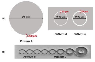
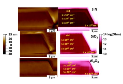
Mask comparison:Three 50 nm-thick mask materials—SiN, SiO₂, and Al₂O₃—were deposited and patterned before localized GaN growth. Six samples representing two epitaxial structures and the three mask materials were investigated.
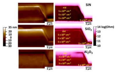
Calibration structure:One set of samples contained GaN layers with nominal Si-doping concentrations of 5 × 10¹⁸ cm⁻³, 5 × 10¹⁷ cm⁻³, and 5 × 10¹⁶ cm⁻³, together with a nominally undoped layer. These layers served as internal references for interpreting the SSRM response.
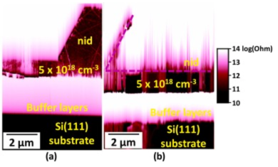
SSRM characterization:Top-view and cross-sectional SSRM measurements were performed using a Bruker Dimension ICON AFM equipped with doped-diamond-coated conductive probes. The technique measured local spreading resistance, which is related to the local resistivity and carrier concentration of the GaN.
Measurement conditions:Depending on the sample and measurement geometry, DC sample biases of −2 V, −6 V, or −8 V were applied between the conductive probe and the back contact.
Independent verification:SIMS measurements were used to determine the concentrations of silicon, oxygen, and carbon and to verify the trends observed through SSRM.
3. Key Findings
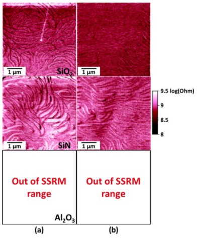
Strong mask-dependent doping:GaN grown using SiN and SiO₂ masks exhibited high unintentional doping. In several regions, the carrier or impurity concentration was on the order of 10¹⁸ cm⁻³, which is too high for the drift region of high-voltage vertical GaN devices.
Superior performance of Al₂O₃:The Al₂O₃ mask produced much more resistive GaN. SSRM clearly distinguished the intentionally doped layers, while the nominally undoped layer exhibited extremely high resistance.
Record-low unintentional doping:SIMS measurements supported the SSRM results and showed a silicon concentration as low as approximately 5 × 10¹⁵ cm⁻³ in the nominally undoped GaN grown with the Al₂O₃ mask. The combined results indicate a carrier concentration below 1 × 10¹⁶ cm⁻³.
Extension of SSRM capability:According to the authors, this is the first demonstration that SSRM can image GaN layers with doping concentrations on the order of 10¹⁶ cm⁻³.
Progress toward vertical GaN devices:Crack-free localized GaN structures with thicknesses of approximately 6–7 μm were obtained. Although still below the approximately 10 μm target, the results represent an important step toward GaN-on-Si drift layers for 1200 V vertical power devices.
Chinese text arrangement
The research revolves around the low-doping drift layer required for vertical power devices using gallium nitride on silicon (GaN-on-Si). The researchers performed local selective epitaxy of GaN on a 200 mm silicon wafer and compared the effects of three mask materials, SiN, SiO₂ and Al₂O₃, on unintentional doping of GaN.
Experimental results show that when using SiN or SiO₂ as an epitaxial mask, silicon and related impurities in the mask may enter GaN during the diffusion and epitaxial growth of Ga atoms, bringing the unintentional doping concentration to approximately 10¹⁸ cm⁻³. This doping level will make the drift layer resistance too low to meet the requirements of high-voltage vertical GaN power devices.
In contrast, the Al₂O₃ mask can significantly reduce the introduction of silicon impurities. SSRM measured that the corresponding GaN layer had high local resistance, and SIMS further confirmed that its unintentional doping concentration was lower than 1 × 10¹⁶ cm⁻³, and the silicon concentration in some areas was approximately 5 × 10¹⁵ cm⁻³.
The study also obtained a GaN local epitaxial structure with a thickness of nearly 7 μm and no cracks on the surface, which provides an experimental basis for further preparation of a drift layer about 10 μm thick and suitable for 1200 V-level vertical power devices.
[The core use of SSRM in this research]
Two-dimensional local resistance and doping distribution imaging
SSRM uses a conductive probe to scan the GaN surface or cross-section and measure the local extended resistance under the probe. Since the expansion resistance is closely related to the local resistivity and carrier concentration of the material, researchers can visually compare the doping differences in different epitaxial layers and different locations.
Comparing the contamination effects of three mask materials
By conducting SSRM measurements on SiN, SiO₂ and Al₂O₃ samples under the same conditions, the researchers found that the resistance at the edges and epitaxial layers of the SiN and SiO₂ samples was significantly lower, indicating the presence of strong unintentional doping; while the Al₂O₃ sample showed higher resistance and clear interlayer differences.
Analyze the longitudinal doping structure inside the epitaxial layer
Cross-sectional SSRM is able to display GaN layers at different depths simultaneously. The researchers used a GaN layer of known doping concentration as an internal calibration reference to determine the resistance and carrier concentration of the nominally undoped layer and observe how doping changes with epitaxial layer depth.
Verifying the scalability of low-doped GaN
The study applies SSRM to GaN layer imaging with a doping concentration of about 10¹⁶ cm⁻³ for the first time, expanding the practical measurement range of this technology in high-resistance wide-bandgap semiconductors.
Complementary verification with SIMS
SSRM provides local electrical distribution information with high spatial resolution, while SIMS provides concentration depth information of elements such as Si, O, and C. The combination of the two can link "local conductivity changes" with "sources of impurities" to improve the reliability of judgments on epitaxial process problems.
[Technical contribution and value]
Provide direct basis for GaN epitaxial process screening
Research has proven that Al₂O₃ is more suitable than SiN and SiO₂ as a mask material for low-doped GaN local epitaxy. This conclusion can directly guide the material and process development of vertical GaN power devices.
Establish the connection between process, doping profile and device performance
The doping concentration of the drift layer directly affects the withstand voltage, leakage and on-resistance of the power device. SSRM can locate abnormally conductive areas before device fabrication, so epitaxial quality assessment is no longer limited to large-area average measurements.
Promote the expansion of SSRM to low-doping analysis of wide-bandgap semiconductors
GaN surface oxide layer, contact characteristics and high resistance all increase the difficulty of SSRM measurement. This study proves that SSRM can be used for GaN doping analysis at the 10¹⁶ cm⁻³ level through cross-validation of doped reference layers, conductive diamond probes and SIMS.
Support high-voltage vertical GaN-on-Si device development
The carrier concentration below 1 × 10¹⁶ cm⁻³ and the crack-free GaN structure of about 7 μm indicate that the local epitaxial route is close to the thick drift layer and low doping requirements required for 1200 V-level vertical devices.
[Measurement limitations]
The SSRM signal is not only affected by the carrier concentration, but also by the probe contact area, surface topography, oxide layer and cross-section polishing damage. Therefore, the absolute quantitative capability of SSRM in this study is still limited, and some results need to rely on known doped layers for calibration and be verified by SIMS. Its outstanding advantages mainly lie in high spatial resolution two-dimensional electrical imaging and relative comparison between different samples.
Original link:

